TRI's ground breaking 3D AOI solution delivers the fastest hybrid PCB inspection combining optical and blue-laser-based true 3D profile measurement for the highest automated defect symptom coverage possible. Integrated state-of-the-art software solution and third generation intelligent hardware platform offer stable and robust 3D solder and component defect inspection and with high inspection coverage and easy programming.
AOI Key Features
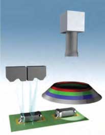
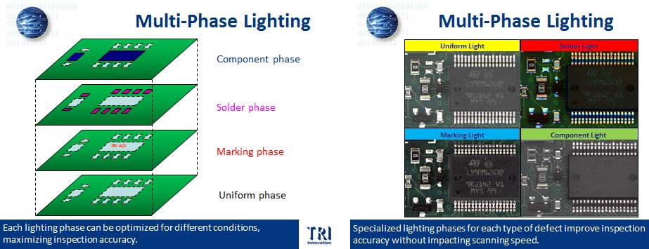
Multi-phase Lighting
Four individual lighting phases improve inspection of individual defect types using specialized lighting conditions. High speed camera allows inspection at constant speed even with multiple lighting phases.
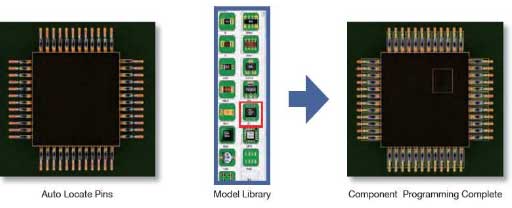
Auto Library + Model Library
Auto Library speeds up programming by automatically allocating inspection windows for IC leads.
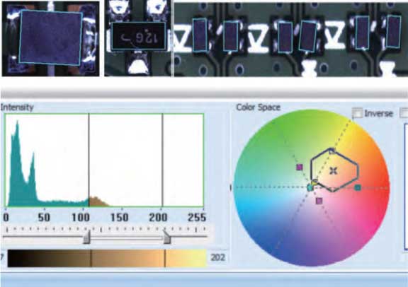
New Color Space Algorithms
TRI's new adaptive algorithms use color space processing to increase inspection accuracy,reduce false calls and improve inspection results while reducing time necessary for inspection fine tuning and the number of alternative images required.